SBS Bit3 PCI to VME Adapter

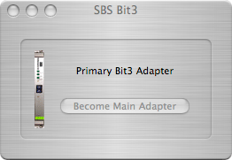

If more than one Bit3 adapter is in the crate you must select one of them to be the main adapter. Any others become placeholders

It produces no data.
Here’s its dialog:
The jumpers on the Bit 3 board must set up correctly for VME accesses to work. If you are getting VME exceptions during read/write operations, it may be that the jumpers on the board are incorrect. The jumper setting for using the Bit 3 board without an eCPU are as follows:
-
• J12: should only have jumper across #4.
-
• J3: should only have jumper across #2, 3, 4, 5 only. #1, 6 & 7 should be open.
-
• J11: all open.
-
• J4: jumper across #3 only.
-
• J2: (looking from the 0 label there are 4 pins across. #'s 0, 1, & 2 should have pins 2 & 3 jumpered. #3 should have pins 1 & 2 jumpered and pins 3 & 4 jumpered. The last row of this connector is labeled on the end ARB and P/R. ARB should be jumpered and P/R should be open.
-
• J9: all should be jumpered EXCEPT #13 HI.
-
• J10: all should be jumpered EXCEPT #13 LO.
-
• J13: all should be jumpered.
-
• J14: all should be jumpered EXCEPT 31 and A24 (A24 is on the right side of 16 as you are looking at the board, it is the end set of pins on the opposite end of 31).
-
• J5: all should be jumpered.
-
• J6: all should be jumpered EXCEPT 31 and A24 (A24 is on the right side of 16 as you are looking at the board, it is the end set of pins on the opposite end of 31).
-
• J8: all open.
-
• J7: all should be jumpered. These are 3 pin sets, the pins that should be jumpered are the middle pin and the pin closest to the pin numbering (or closest to the VME connector).
The jumper setting for using the Bit 3 board with an eCPU and dual port memory are as follows:
-
• J12: should be all open.
-
• J3: should only have jumper across # 3, 5 only. #1, 2, 4, 6 & 7 should be open.
-
• J11: all open.
-
• J4: jumper across #3 only.
-
• J2: (looking from the 0 label there are 4 pins across. #'s 0, 1, & 2 should have pins 2 & 3 jumpered. #3 should have pins 1 & 2 jumpered and pins 3 & 4 jumpered. The last row of this connector is labeled on the end ARB and P/R. Both ARB and P/R should be open.
-
• J9: all should be jumpered EXCEPT #13 HI.
-
• J10: all should be jumpered EXCEPT #13 LO.
-
• J13: all should be jumpered ECCEPT #23,27.
-
• J14: all should be jumpered EXCEPT 27 and A24 (A24 is on the right side of 16 as you are looking at the board, it is the end set of pins on the opposite end of 31).
-
• J5: all should be jumpered.
-
• J6: all should be jumpered EXCEPT 31 and A24 (A24 is on the right side of 16 as you are looking at the board, it is the end set of pins on the opposite end of 31).
-
• J8: all open.
-
• J7: all should be jumpered. These are 3 pin sets, the pins that should be jumpered are the middle pin and the pin closest to the pin numbering (or closest to the VME connector).