CAEN V265

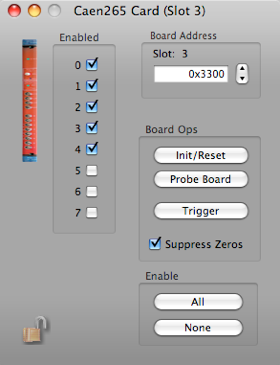

Set the VME Address

Please refer to the manual for more details.
V265 Data Record format
The ADC data from the V265 can be in either the short or the long form. The short form will be used whenever possible, but analysis programs must be prepared to handle either form.
Short Form:
xxxx xxxx xxxx xxxx xxxx xxxx xxxx xxxx
^^^^ ^^--------------------------------- V265 ID (from header)
--------^-^^^--------------------------- Crate number
-------------^-^^^^--------------------- Card number
--------------------^^^----------------- Channel number
-----------------------^---------------- Range Type (0==12 bit, 1==15bit)
-------------------------^^^^ ^^^^ ^^^^- adc value
Long Form:
xxxx xxxx xxxx xxxx xxxx xxxx xxxx xxxx
^^^^ ^^^^ ^^^^ ^^----------------------- V265 ID (from header)
-----------------^^ ^^^^ ^^^^ ^^^^ ^^^^- length (always 2 longs)
xxxx xxxx xxxx xxxx xxxx xxxx xxxx xxxx
--------^-^^^--------------------------- Crate number
-------------^-^^^^--------------------- Card number
--------------------^^^----------------- Channel number
-----------------------^---------------- Range Type (0==12 bit, 1==15bit)
-------------------------^^^^ ^^^^ ^^^^- adc value


Force ALL/NONE of the channels to be enabled
Option to exclude ADC values that are zero from the data stream
ADC values from channels that are not enabled will be dumped and not included in the data stream.

Force a Gate signal

Reset the board and clear the FIFO