LBL Gretina4


Flush all data from the FIFO

Each channel of the board can be independently triggered and three triggering modes are provided; internal, external and validate modes. In internal mode a channel of the signal processing board is triggered by an internal, digitally implemented, leading edge discriminator. Each discriminator is accessible as an ECL logic pulse at the front panel. In external mode, the channel is triggered by an externally provided ECL logic pulse input on the boards front panel. In validate mode, the board is triggered if the leading edge discriminator fires followed by an externally provided ECL logic signal which validates the event.
Associated with each event produced by a valid trigger is a 48 bit time stamp, incremented at the digitization rate,which allows for event building between digitizer boards. Each board can be configured to operate from an external clock to synchronize these time stamps.
Each board contains a 1 MB output FIFO to store events before they are read out. These events contain an event header (which includes the energy, leading edge and constant fraction time, segment and board ID) and a section of the trace from the triggered channel. Mechanisms to support both polled and interrupt driven acquisition systems are provided. Board configuration is also done over the VME backplane where the integration time for the energy, the position of the trace windows, discriminator levels and constant fraction discriminator parameters can be set.
See the manual for more specific information.
Firmware
The correct version of firmware to be running with this card is v1.06 for the main FPGA and v32-41 (April 17,2013) for the VME FPGA. Previous version of the VME firmware have an issue that prevents the GRETINA card from existing simultaneously in a crate with A16/A24 cards. The newer version of the firmware fixes that problem.
The newest version of the VME firmware is available here: gr-vme-v32-41Works.mcs.
v1.06 of the main firmware is available here: chip_top_1.06_0039.bin.
download the lab tools from here:
-
• Connect the Platform Cable to the JTAG header on the Gretina card and to a computer with the Lab Tools installed . Put the card in a VME crate and power it on.
-
• Start the Xilinx iMpact software, open a boundary scan, and initialize the data chain. iMpact should detect the Platform cable and two chips.
-
• Right-click on the image of the chip labeled xcf02s. This is the VME FPGA. Click the 'assign new configuration file' option and select VME firmware file. Right-click on the image of the chip and click 'program'.
-
• When the programming is complete, power-cycle the crate. You are now running the new VME firmware.
-
• In the ORCA GRETINA dialog, select the ‘Firmware’ tab and download the main FPGA .bin file that is available above. It takes awhile. Be patient.


Run an algorithm to set the thresholds of enabled channels to the noise floor
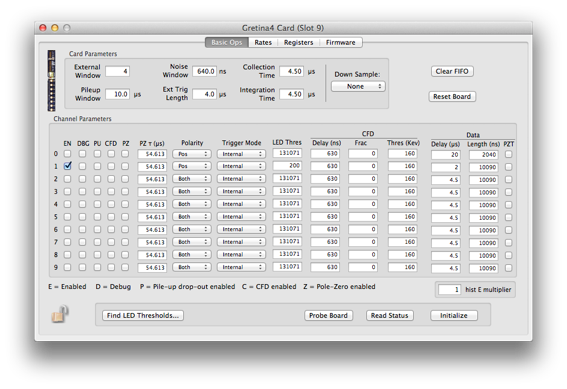
Parameters common to all channels


Threshold and triggering parameters

Write all values to the hardware
Helpful Hint.
Use Cmd-Shift-> and Cmd-Shift-< to make this dialog control a card in a slot to the right or left of the currently selected card.
Use Cmd-C to bring up another card dialog, set one of them to the Rates display and one to the Settings display to see rates while setting thresholds.

Various set-up flags. Only enabled channels will be read out.


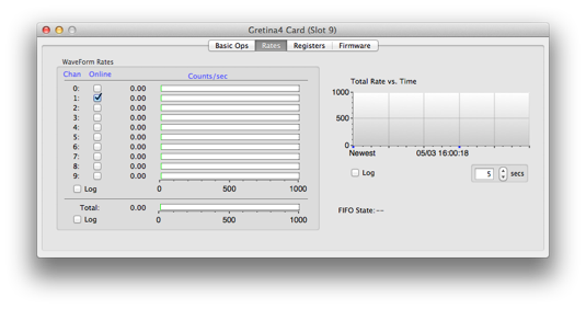
Rate over time.
Current FIFO state information
Channel-by-channel rates. Note that you can enable/disable channels here also
Waveform record:
xxxx xxxx xxxx xxxx xxxx xxxx xxxx xxxx
^^^^ ^^^^ ^^^^ ^^----------------------- Data ID (from header)
-----------------^^ ^^^^ ^^^^ ^^^^ ^^^^- length
xxxx xxxx xxxx xxxx xxxx xxxx xxxx xxxx
--------^-^^^--------------------------- Crate number
-------------^-^^^^--------------------- Card number
xxxx xxxx xxxx xxxx xxxx xxxx xxxx xxxx
------------------------------------^^^- Channel number
^^^^ ^^^^ ^^^^ ^^^^--------------------- Data Length
xxxx xxxx xxxx xxxx xxxx xxxx xxxx xxxx
--------------------^^^^ ^^^^ ^^^^ ^^^^- LED1
^^^^ ^^^^ ^^^^ ^^^^--------------------- LED2
xxxx xxxx xxxx xxxx xxxx xxxx xxxx xxxx
--------------------^^^^ ^^^^ ^^^^ ^^^^- LED3
^^^^ ^^^^ ^^^^ ^^^^--------------------- Energy bit 0-15
xxxx xxxx xxxx xxxx xxxx xxxx xxxx xxxx
-------------------------------^^^ ^^^^- Energy bit 16-22
--------------------^------------------- P
---------------------^------------------ C
----------------------^----------------- E
-----------------------^---------------- Sx
^^^^ ^^^^ ^^^^ ^^^^--------------------- CFD Timestamp bit0-15
xxxx xxxx xxxx xxxx xxxx xxxx xxxx xxxx
--------------------^^^^ ^^^^ ^^^^ ^^^^- CFD Timestamp bit16-31
^^^^ ^^^^ ^^^^ ^^^^--------------------- CFD Timestamp bit32-47
xxxx xxxx xxxx xxxx xxxx xxxx xxxx xxxx
------------------------ ^^^^ ^^^^ ^^^^- Raw data point0
-----^^^^ ^^^^ ^^^^--------------------- Raw data point1
Raw data points continue until the Data length is used up....