LBL Gretina4 (MJD)


Flush all data from the FIFO

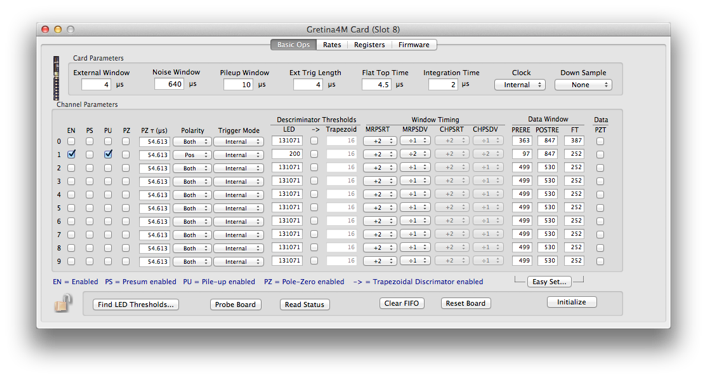
Each channel of the board can be independently triggered and three triggering modes are provided; internal, external and validate modes. In internal mode a channel of the signal processing board is triggered by an internal, digitally implemented, leading edge discriminator. Each discriminator is accessible as an ECL logic pulse at the front panel. In external mode, the channel is triggered by an externally provided ECL logic pulse input on the boards front panel. In validate mode, the board is triggered if the leading edge discriminator fires followed by an externally provided ECL logic signal which validates the event.
Associated with each event produced by a valid trigger is a 48 bit time stamp, incremented at the digitization rate,which allows for event building between digitizer boards. Each board can be configured to operate from an external clock to synchronize these time stamps.
Each board contains a 1 MB output FIFO to store events before they are read out. These events contain an event header (which includes the energy, leading edge and constant fraction time, segment and board ID) and a section of the trace from the triggered channel. Mechanisms to support both polled and interrupt driven acquisition systems are provided. Board configuration is also done over the VME backplane where the integration time for the energy, the position of the trace windows, discriminator levels and constant fraction discriminator parameters can be set.
See the Gretina4Manual.pdf for more specific information about the original card and Gretina1_07.pdf for details of the new version. As of April 2014, version 3.0 of the firmware is the version to use. There are still some problems with corrupted headers.
Firmware
The correct version of firmware to be running with this card is v1.07 for the main FPGA and v32-41 (April 17,2013) for the VME FPGA. Previous version of the VME firmware have an issue that prevents the GRETINA card from existing simultaneously in a crate with A16/A24 cards. The newer version of the firmware fixes that problem.
The newest version of the VME firmware is available here: gr-vme-v32-41.mcs.
v3.0 of the main firmware is available here: chipmj_top_3.00_10000037.bin.
Download the lab tools from here:
-
• Connect the Platform Cable to the JTAG header on the Gretina card and to a computer with the Lab Tools installed . Put the card in a VME crate and power it on.
-
• Start the Xilinx iMpact software, open a boundary scan, and initialize the data chain. iMpact should detect the Platform cable and two chips.
-
• Right-click on the image of the chip labeled xcf02s. This is the VME FPGA. Click the 'assign new configuration file' option and select VME firmware file. Right-click on the image of the chip and click 'program'.
-
• When the programming is complete, power-cycle the crate. You are now running the new VME firmware.
-
• In the ORCA GRETINA dialog, select the ‘Firmware’ tab and download the main FPGA .bin file that is available above. It takes awhile. Be patient.
-
• NOTE: if there are problems loading the firmware, see the bottom of this page for more info.


Run an algorithm to set the thresholds of enabled channels to the noise floor
Parameters common to all channels


Threshold and triggering parameters

Write all values to the hardware
Helpful Hint.
Use Cmd-Shift-> and Cmd-Shift-< to make this dialog control a card in a slot to the right or left of the currently selected card.
Use Cmd-C to bring up another card dialog, set one of them to the Rates display and one to the Settings display to see rates while setting thresholds.

Various set-up flags. Only enabled channels will be read out.


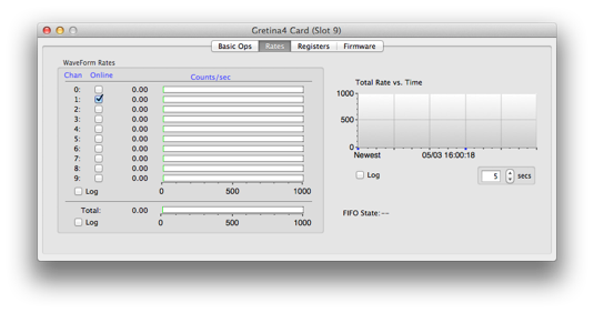
Rate over time.
Current FIFO state information
Channel-by-channel rates. Note that you can enable/disable channels here also
Waveform record:
xxxx xxxx xxxx xxxx xxxx xxxx xxxx xxxx
^^^^ ^^^^ ^^^^ ^^----------------------- Data ID (from header)
-----------------^^ ^^^^ ^^^^ ^^^^ ^^^^- length
xxxx xxxx xxxx xxxx xxxx xxxx xxxx xxxx
--------^-^^^--------------------------- Crate number
-------------^-^^^^--------------------- Card number
xxxx xxxx xxxx xxxx xxxx xxxx xxxx xxxx
^^^^ ^^^^ ^^^^ ^^^^ ^^^^ ^^^^ ^^^^ ^^^^ always 0xAAAAAAAA
xxxx xxxx xxxx xxxx xxxx xxxx xxxx xxxx
------------------------------------^^^- Channel number
--------------------^^^^ ^^^^ ^^^^------ Board ID
^^^^ ^^^^ ^^^^ ^^^^--------------------- Always 0x0000
xxxx xxxx xxxx xxxx xxxx xxxx xxxx xxxx
^^^^ ^^^^ ^^^^ ^^^^ ^^^^ ^^^^ ^^^^ ^^^^- LED timestamp
xxxx xxxx xxxx xxxx xxxx xxxx xxxx xxxx
--------------------^^^^ ^^^^ ^^^^ ^^^^- LED timestamp
^^^^ ^^^^ ^^^^ ^^^^--------------------- Energy
xxxx xxxx xxxx xxxx xxxx xxxx xxxx xxxx
--------------------^^^^ ^^^^ ^^^^ ^^^^- Energy
^^^^ ^^^^ ^^^^ ^^^^--------------------- CFD Timestamp
xxxx xxxx xxxx xxxx xxxx xxxx xxxx xxxx
--------------------^^^^ ^^^^ ^^^^ ^^^^- CFD Timestamp
^^^^ ^^^^ ^^^^ ^^^^--------------------- CFD Timestamp
xxxx xxxx xxxx xxxx xxxx xxxx xxxx xxxx
--------------------^^^^ ^^^^ ^^^^ ^^^^- CFD1 L
^^^^ ^^^^ ^^^^ ^^^^--------------------- CFD1 H
xxxx xxxx xxxx xxxx xxxx xxxx xxxx xxxx
--------------------^^^^ ^^^^ ^^^^ ^^^^- CFD2 L
^^^^ ^^^^ ^^^^ ^^^^--------------------- CFD2 H
xxxx xxxx xxxx xxxx xxxx xxxx xxxx xxxx - Word 16, 17 Reserved
xxxx xxxx xxxx xxxx xxxx xxxx xxxx xxxx - Word 18, 19 Reserved
xxxx xxxx xxxx xxxx xxxx xxxx xxxx xxxx - Word 20, 21 Reserved
xxxx xxxx xxxx xxxx xxxx xxxx xxxx xxxx - Word 22, 23 Reserved
xxxx xxxx xxxx xxxx xxxx xxxx xxxx xxxx - Word 24, 25 Reserved
xxxx xxxx xxxx xxxx xxxx xxxx xxxx xxxx - Word 26, 27 Reserved
xxxx xxxx xxxx xxxx xxxx xxxx xxxx xxxx - Word 28
--------------------^^^^ ^^^^ ^^^^ ^^^^- Reserved
^^^^ ^^^^ ^^^^ ^^^^--------------------- First Data Word
....1009 Long Words of Raw data points follow.....
Recovering from Firmware Problems
If the GRETINA cards are not working properly and all of the lights on the front of the card are yellow, you will have to try to reinstall the firmware or change the fuses on the board. Due to some compatibility problems with the newest firmware, a fresh install of the newest firmware (v1.07) for the GRETINA cards may not allow you to communicate with the GRETINA card via ORCA. As such, here we provide a guide for getting the new firmware working:
1) Using the Xilinx Lab Tools ISE iMPACT software and the XILINX Platform Cable USB II, connect the computer to the side of the GRETINA card (JTAG port).
2) In the iMPACT software, choose Boundary Scan and then click Initialize Chain to find the devices you’re connected to.
3) The first device (on the left) should read something like xcf02s, right click it and choose Assign New Configuration File.
4) Here choose the vme-28-41.mcs file for the configuration file and then right click the device and choose Program. This should install an older version of the VME firmware on the GRETINA card.
5) Here you need to turn off the VME crate to restart the card for the installation to set. Do this now; don’t forget to shutdown the SBC first.
6) Now the second device (on the right) should read something like xc3s5000, right click it and choose Assign New Configuration File.
7) This time choose the chip_top_001_05b.bit file as your configuration file. Then right click on the device and choose Program. This should install an older version of the main FPGA firmware for use of the GRETINA card with ORCA. This time don’t turn off the VME crate, the firmware you’ve just installed will be deleted if you turn the crate off now.
8) From here, you should be able to talk to the card using ORCA in the normal fashion (put it in a VME crate with an SBC and connect). It may tell you it has outdated firmware, this is OK.
9) Now in the ORCA dialog for the GRETINA card there should be tab labeled Firmware if there isn’t, update ORCA. Choose this tab and click Load to install the newest version of the main FPGA firmware on the GRETINA card. For this option, you should use the newest version on the ORCA help site mentioned above, as of April 2014 this is chipmj_top_3.00_10000037.bin, download it from the help site if you don’t have it.
10) Now that you’ve finished installing the new main FPGA firmware, you will need to update to the newest VME firmware for the GRETINA card.
11) To do this, go back to the XILINX lab tools and find the devices, choose the first device (xcf02s) and right click Assign New Configuration File and this time choose the newest VME firmware available on the ORCA help site mentioned above, as of November, 2013 this is gr-vme-v32-41Works.mcs. Now just click Program and it should install the new VME firmware on the card.
12) Here just restart the VME crate and you should be able to use the card properly with ORCA and it now has all of the new firmware installed on it.
Additional Notes:
· Turning off the VME crate will erase the main FPGA firmware you installed using XILINX but not the main FPGA firmware you installed using ORCA.
· None of these steps should take more than 10-20 minutes; if ORCA is taking forever to load the main FPGA firmware something may be wrong.
· The GRETINA card must be plugged into a powered VME crate for the XILINX software to read it and install firmware on it.